O2 Sensor Display Board
Component List
- 1 Green LED 1.8v
- 1 Red LED 1.8v
- 1 Yellow LED 1.8v
- 1 LM324N IC: Max Pd = 1310mW, Max operating Temp: -25 ~ +85°C
- 4 IN4001 Diodes
- 1 9V1 Zener diode
- 4 470Ω Resistors
- 1 10KΩ Resistor
- 1 390Ω Resistor
- 1 270Ω Resistor
- 2 0.1uF Capacitors
- Jumper Wires
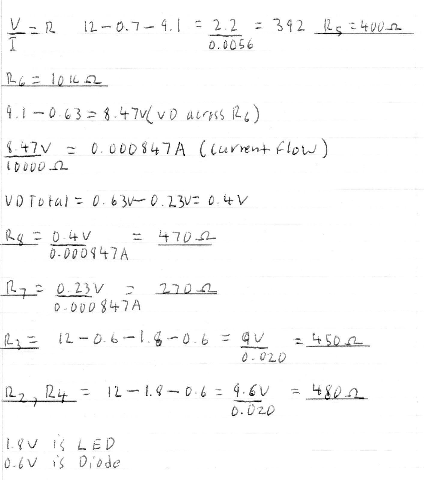
Calculations
 Technical Explanation
This circuit is designed to show an Oxygen sensors voltage reading, which it obtains from the air fuel mixture after combustion.
It does this by lighting up a red, green or yellow LED to show the conditions of the air fuel mixture.
It uses a IC Chip (integrated Circuit) Called the LM324 Comparator. This comparator compares voltage from the oxygen sensor to a pre-set voltage caused by the resistors on the board.
Basically the series resistors have two voltages which it uses to compare with the O2 sensors voltage. This is between 0.23V and 0.63V.
The list below explains what the different coloured LEDs represent when they are lit:
- Less than 0.23V: Green. Air fuel ratio is lean
- Between 0.23V and 0.63V: Yellow. Air fuel ratio is said to be stoich (14.7:1) which is optimum mixture
- Above 0.63V: Red. Mixture is said to be rich
Reflection
I had a bit of trouble getting the circuit working because of not wiring the chip up correctly and a faulty Yellow LED. But once these problems were diagnosed and repaired it began working correctly.
If I was to build this circuit again I would probably make the layout more simpler so that wiring it up is a lot easier and fault diagnosing is easily performed.
By doing this circuit I learned how to wire up vera boards correctly and also how to find out problems with it. I also learned to be very careful with how I soldier the circuit and to check everything over each time a new part is added and soldiered to the board.
 |
| Bread Board Design |
 |
| Loch Master Design |
 |
| Vera Board Design |
 |
| Vera Board Soldiering |


